Table of Contents
V6Z80P Plus V1.1 Hardware overview
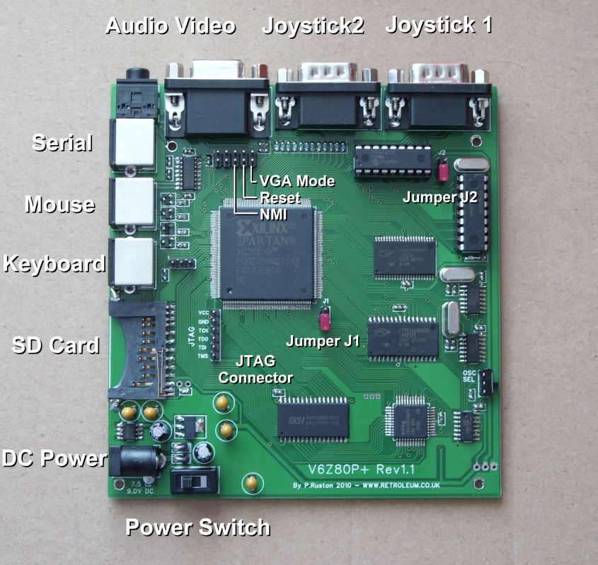
V6Z80P+ V1.1 Brief circuit description
The V6Z80P system is based on a Spartan 2 FPGA (XC2S150) and 20MHz Z80 CPU (normally) running at 16MHz.
The V1.1 version of the board allows the CPU clock to be driven by a signal from the FPGA and there are footprints allowing other oscillators to be mounted (74HC04+crystal or 3.3v SMT 7x5mm oscillator).
FPGA configuration is handled by a PIC chip which uses a 20MHz crystal. There is also another PIC acting as a parallel-to-serial joystick interface - this uses its own internal 4MHz clock.
Memory buses
- “Video memory” - 512KB 10ns 3.3 volts, direct connection. Chip always selected.
- “Sprite memory” - 128KB 10ns 3.3 volts, direct connection. Chip always selected.
- “System memory” - 512KB 25ns 5 volts. Signals D0-D7, A0:A13, /RD and /WR are routed direct to the relevent Z80 pins (and also FPGA pins). System RAM lines A18:14 and /CS are connected only to the FPGA. Z80 A15:14 are connected (only) to the FPGA - this allows the Z80 address space to be paged in 16KB chunks. (For original V6Z80P compatibility, OSCA loops A14 straight through the FPGA from the Z80 to system RAM, page granularity is therefore 32KB under OSCA)
CPU connections
All Z80 control pins (except from RFSH and HALT which arent used) are connected to FPGA pins (and some to System RAM, see above). As mentioned, the Clock input is routed via a 74HCT08 chip which mainly acts as a 3.3 to 5.0 volt voltage shifter (due the Z80's clock line requirements)
V6Z80P Plus Peripherals
The following diagrams show how various external circuits (peripheral connectors etc) are connected to the V6Z80P+'s Spartan 2 FPGA
V6Z80P Plus Joystick

V6Z80P Plus V1.1 PIC and EEPROM

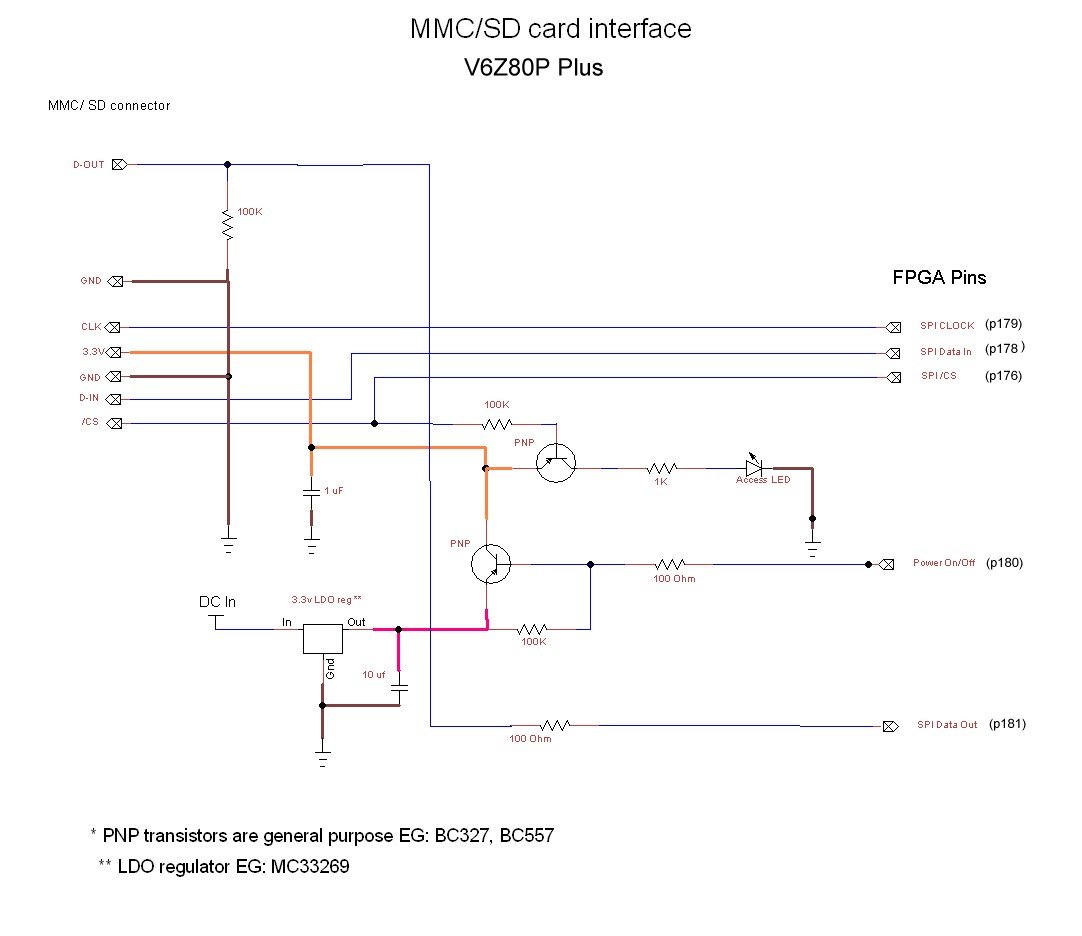
V6Z80P Plus SD card interface schematics
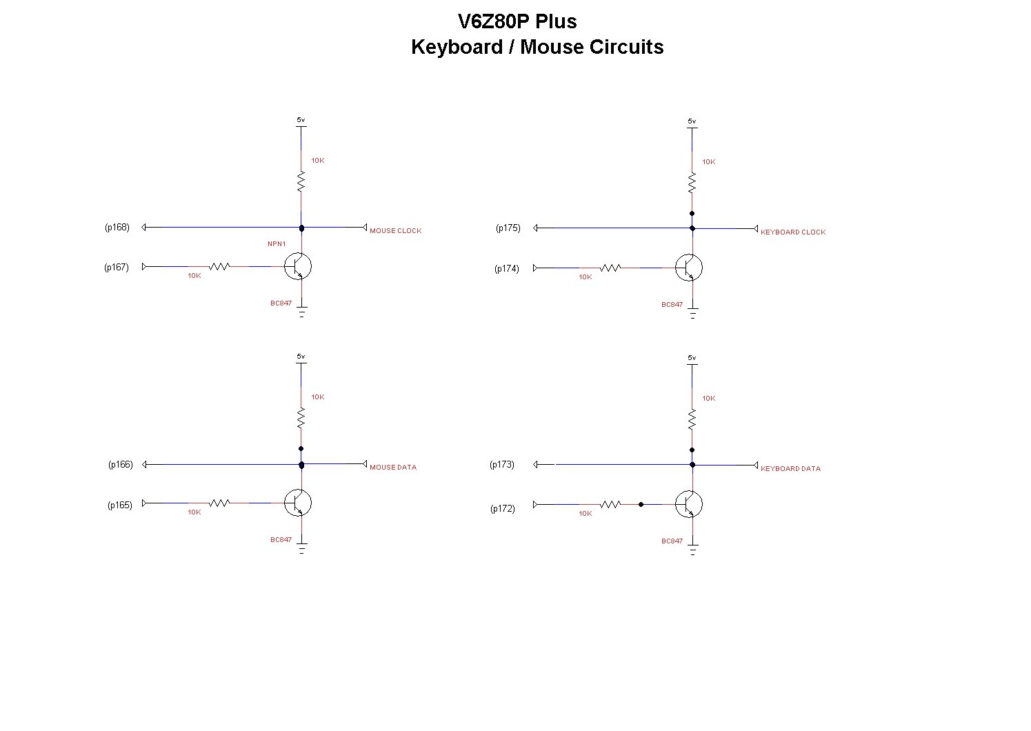
V6Z80P Plus Keyboard and mouse schematics
V6Z80P Plus Audio and video schematics

V6Z80P Plus Serial comms schematics

V6Z80P V1.1 Clock routing

V6Z80P V1.1 Plus Complete Spartan2 Pin Out List
Audio
Two outputs from the FPGA (Sigma/Delta pulse trains) drive a simple resistor/capacitor filter. The output of which has its amplitude halved by a potential divider (2 x 10K), passed via 1uf capacitor to the left and right of the audio socket.
Serial Port
To connect to a standard RS232 serial port - RX and TX only are implemented. The lines are routed via a ST232 level converter chip to and from the FPGA.

Video Port
12 FPGA ouputs drive 3 x 4 resitor DACs, this allows a palette of 4096 colours. The RGB levels are <0.7v suitable for TV for VGA monitor. 2 additional FPGA outputs drive Horizontal and Vertical sync - these are both passed through 100 ohm resistors. These outputs will directly drive a PC monitor, and can be used to drive a TV's RGB inputs with a simple adapter cable (All lines are connected direct the relevant SCART pins, with the exception of V_sync which is passed though two 330 Ohm resistors in series, adjusting the voltage to that required by composite sync. The horizontal sync is connected to the SCART “blanking” input - when the system is in TV mode, the line is driven permanently high which activates RGB mode in the TV).

PS2 ports
Keyboard and mouse. CLOCK and DATA directly connected to FPGA. These lines can also be pulled down (for output) on the V6Z80P side by transistors connected to the FPGA. (8 FPGA pins used in total).
Joystick
Two ATARI 2600 style connectors: 6 inputs each. Also compatible with the original Megadrive pads. Lines are pulled up by resistors on the PCB and pulled low by the switches in the joystick. The 12 lines are connected to a PIC 16F62x microcontroller which acts as a parallel-to-serial converter. Two FPGA pins for Clock and Data are used to read the joystick data.
MMC/SD memory card
Uses 5 FPGA pins to connect to Power, /Card Select, Data_in, Data_out and Clock. /Card select is also connected to an LED via resistor for access indication. The FPGA /Power line switches a PNP transistor to apply power to the card.
Other pins connected to the FPGA
There are 5 pins available to use for external connections via a pin header near the video socket. (In OSCA, 3 of these pins are used for video type select, reset and NMI inputs, the other 2 are free I/O ports.)

The configuration system uses several FPGA pins to upload config and communicate with the PIC controller dedicated to this task (includes reprogramming the EEPROM etc).
JTAG port
Used for “live” config of the FPGA, standard Xilinx pin out sequence.
Config selection jumper
Selects between JTAG mode and normal EEPROM config (slave serial mode)